India wants to make its own microchips, and it just got the ultimate tool to do it.
If you follow the tech world, you know that building a semiconductor fabrication plant, or a "fab," is one of the most complex engineering challenges on Earth. You can't just buy a building, install some machinery, and start printing silicon. You need specialized hardware that only a handful of companies can build.
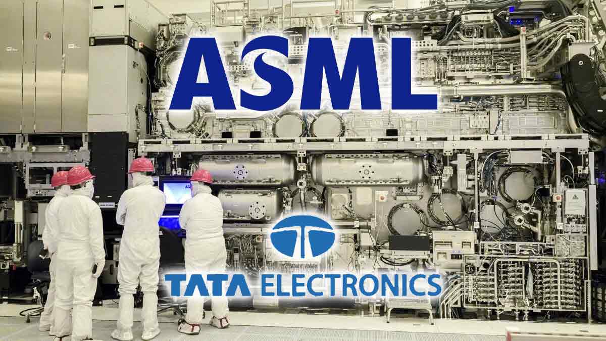
Tata Electronics just secured the biggest name in the business.
During a state visit to the Netherlands, Indian Prime Minister Narendra Modi and Dutch Prime Minister Rob Jetten stood by as Tata Electronics signed a massive Memorandum of Understanding (MoU) with ASML. ASML is the absolute king of lithography equipment. This deal isn't just a basic purchase order. It is a full-scale partnership designed to kickstart, scale, and secure India's first commercial 300 mm semiconductor fab in Dholera, Gujarat.
If you think this is just another corporate press release, you're missing the bigger picture. This agreement changes the timeline for India's tech sovereignty.
[Image of hydrogen fuel cell]
What ASML Brings to Gujarat
To understand why this matters, you have to look at what ASML actually does. In the semiconductor world, lithography is the process of using light to print microscopic patterns onto silicon wafers. ASML builds the complex machines that make this possible. Without their tools, modern computing stops.
Tata is pouring $11 billion into its Dholera facility. They aren't going for old, outdated tech either. The fab will produce 300 mm (12-inch) wafers using 28nm, 40nm, 55nm, 90nm, and 110nm nodes. They have already locked in tech transfer deals with Taiwan's PSMC, and they have been signing agreements with giant players like Tokyo Electron, Renesas, and Intel.
But the machines themselves are useless without the brainpower to run them. That is the real meat of this new agreement. ASML is not just shipping crates to Gujarat; they are actively helping to set up the operations and build a local workforce.
The agreement focuses heavily on three things:
- Ramp-up Support: ASML engineers will work to deploy a holistic suite of lithography tools, making sure the Dholera fab starts up without the costly delays that kill new chip plants.
- Talent Pipelines: They are launching deep skill-development programs. Lithography is a highly specialized discipline, and India currently lacks a deep pool of local experts who have worked on these specific machines.
- Research and Development: The two companies are building out R&D infrastructure right inside India. This means local engineers can innovate on-site rather than relying entirely on European or Taiwanese labs.
The Strategy Behind the Deal
Building a chip industry from scratch takes an insane amount of political and financial will. Prime Minister Modi’s presence at the signing ceremony in The Hague shows exactly how high the stakes are. India wants to cut its total reliance on imported silicon, especially for critical sectors like defense, automotive manufacturing, and consumer tech.
Think about the automotive sector. The global chip shortages a few years ago crippled car production worldwide. Tata owns Jaguar Land Rover and is a massive automaker in its own right. By building a domestic supply of 28nm to 110nm chips—the exact legacy nodes used heavily in cars, home appliances, and medical devices—Tata is protecting its own supply chain while positioning itself as a primary supplier for the global market.
Critics might point out that India isn't jumping straight into sub-7nm cutting-edge nodes for the latest smartphones. Honestly, trying to do that on day one would be a disaster. The legacy and mature node market is where the volume is. It is a smart, calculated business strategy. Learn the ropes on 28nm and 55nm, master the yield rates, build the talent pool, and then look toward the ultra-advanced nodes later.
Your Next Steps to Track This Semiconductor Shift
If you are an investor, an engineer, or a tech business leader, you need to watch how this project moves forward over the next 18 months. The theoretical talk is over; the execution phase has started. Here is how you can practically prepare for the shifts this agreement will create:
- Watch the Talent Migration: Keep an eye on new semiconductor engineering curricula and training centers popping up across Indian universities. If you are a hardware engineer, getting certified or trained through these upcoming Tata-ASML initiatives will make you incredibly valuable.
- Evaluate Your Supply Chain: If your business relies on microcontrollers, automotive chips, or power management ICs, start auditing your manufacturing dependencies. Within the next few years, India will emerge as a viable alternative to mainland China and Taiwan for mature nodes.
- Monitor Ancillary Ecosystems: A fab requires a massive network of chemical suppliers, ultra-pure water facilities, and specialized gas distributors. Companies providing these services are going to see massive demand in the Dholera Special Investment Region.
This deal shows that India is no longer just dreaming about silicon independence. By partnering with the one company that controls the printing press of modern technology, Tata is making sure its $11 billion bet has the teeth to succeed.